- 您现在的位置:买卖IC网 > Sheet目录3873 > PIC16CR76T-I/SS (Microchip Technology)IC PIC MCU 8KX14 28SSOP
2007 Microchip Technology Inc.
DS39599G-page 113
PIC18F2220/2320/4220/4320
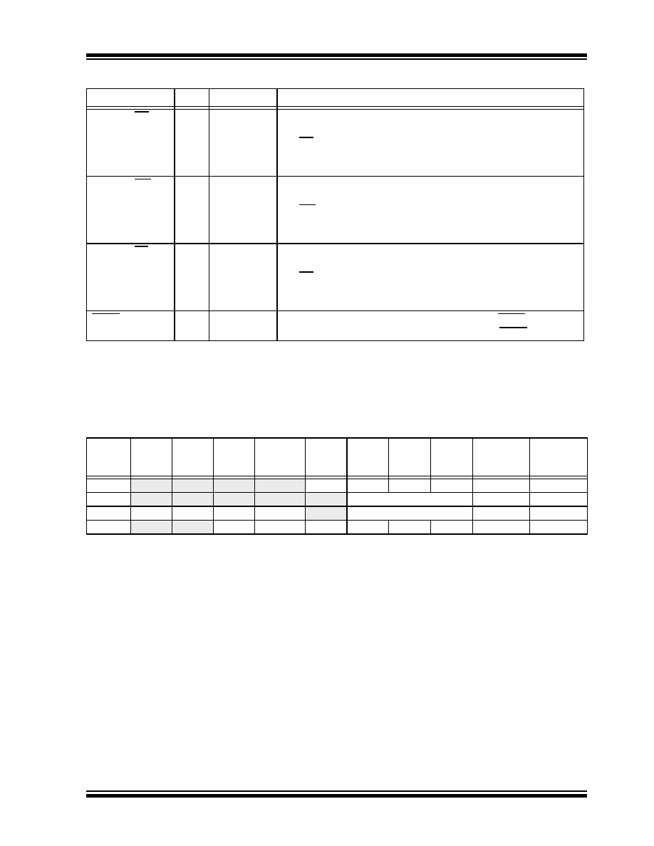
TABLE 10-9:
PORTE FUNCTIONS
TABLE 10-10: SUMMARY OF REGISTERS ASSOCIATED WITH PORTE
Name
Bit#
Buffer Type
Function
RE0/AN5/RD
bit 0
ST/TTL(1)
Input/output port pin, analog input or read control input in Parallel Slave
Port mode.
For RD (PSP Control mode):
1 = PSP is Idle
0 = Read operation. Reads PORTD register (if chip selected).
RE1/AN6/WR
bit 1
ST/TTL(1)
Input/output port pin, analog input or write control input in Parallel
Slave Port mode.
For WR (PSP Control mode):
1 = PSP is Idle
0 = Write operation. Writes PORTD register (if chip selected).
RE2/AN7/CS
bit 2
ST/TTL(1)
Input/output port pin, analog input or chip select control input in Parallel
Slave Port mode.
For CS (PSP Control mode):
1 = PSP is Idle
0 = External device is selected
MCLR/VPP/RE3(2)
bit 3
ST
Input only port pin or programming voltage input (if MCLR is disabled);
Master Clear input or programming voltage input (if MCLR is enabled).
Legend: ST = Schmitt Trigger input, TTL = TTL input
Note 1: Input buffers are Schmitt Triggers when in I/O mode and TTL buffers when in Parallel Slave Port mode.
2: The RE3 port bit is available as an input-only pin only in 40-pin devices and when Master Clear function-
ality is disabled (CONFIG3H<7>=0).
Name
Bit 7
Bit 6
Bit 5
Bit 4
Bit 3
Bit 2
Bit 1
Bit 0
Value on
POR, BOR
Value on
all other
Resets
PORTE
—
—RE3(1)
RE2
RE1
RE0
---- qxxx
---- quuu
LATE
—
LATE Data Latch Register
---- -xxx
---- -uuu
TRISE
IBF
OBF
IBOV
PSPMODE
—
PORTE Data Direction bits
0000 -111
ADCON1
—
VCFG1
VCFG0
PCFG3
PCFG2
PCFG1
PCFG0
--00 0000
Legend:
x = unknown, u = unchanged, - = unimplemented, read as ‘0’, q = value depends on condition.
Shaded cells are not used by PORTE.
Note 1:
The RE3 port bit is available as an input-only pin only in 40-pin devices and when Master Clear functionality is disabled
(CONFIG3H<7>=0).
发布紧急采购,3分钟左右您将得到回复。
相关PDF资料
PIC18F13K50-I/P
IC PIC MCU FLASH 4KX16 20-PDIP
PIC16CR76T-I/SO
IC PIC MCU 8KX14 28SOIC
PIC18LF24K22-I/MV
IC PIC MCU 16KB FLASH 28UQFN
PIC18LF24K22-I/ML
IC PIC MCU 16KB FLASH 28QFN
PIC16CR76T-I/ML
IC PIC MCU 8KX14 28QFN
PIC16F627-04/P
IC MCU FLASH 1KX14 COMP 18DIP
PIC18F45J10-I/ML
IC PIC MCU FLASH 16KX16 44QFN
PIC18F24K22-I/ML
IC PIC MCU 16KB FLASH 28QFN
相关代理商/技术参数
PIC16CR77-I/ML
功能描述:IC PIC MCU 8KX14 44QFN RoHS:是 类别:集成电路 (IC) >> 嵌入式 - 微控制器, 系列:PIC® 16C 产品培训模块:Asynchronous Stimulus
8-bit PIC® Microcontroller Portfolio 标准包装:42 系列:PIC® 16C 核心处理器:PIC 芯体尺寸:8-位 速度:20MHz 连通性:- 外围设备:欠压检测/复位,POR,PWM,WDT 输入/输出数:13 程序存储器容量:3.5KB(2K x 14) 程序存储器类型:OTP EEPROM 大小:- RAM 容量:128 x 8 电压 - 电源 (Vcc/Vdd):4 V ~ 5.5 V 数据转换器:A/D 4x8b 振荡器型:外部 工作温度:-40°C ~ 85°C 封装/外壳:18-SOIC(0.295",7.50mm 宽) 包装:管件 配用:XLT18SO-1-ND - SOCKET TRANSITION 18SOIC 300MILISPICR1-ND - ADAPTER IN-CIRCUIT PROGRAMMING309-1011-ND - ADAPTER 18-SOIC TO 18-DIP309-1010-ND - ADAPTER 18-SOIC TO 18-DIPAC164010-ND - MODULE SKT PROMATEII DIP/SOIC
PIC16CR77-I/P
功能描述:IC PIC MCU 8KX14 40DIP RoHS:是 类别:集成电路 (IC) >> 嵌入式 - 微控制器, 系列:PIC® 16C 产品培训模块:Asynchronous Stimulus
8-bit PIC® Microcontroller Portfolio 标准包装:42 系列:PIC® 16C 核心处理器:PIC 芯体尺寸:8-位 速度:20MHz 连通性:- 外围设备:欠压检测/复位,POR,PWM,WDT 输入/输出数:13 程序存储器容量:3.5KB(2K x 14) 程序存储器类型:OTP EEPROM 大小:- RAM 容量:128 x 8 电压 - 电源 (Vcc/Vdd):4 V ~ 5.5 V 数据转换器:A/D 4x8b 振荡器型:外部 工作温度:-40°C ~ 85°C 封装/外壳:18-SOIC(0.295",7.50mm 宽) 包装:管件 配用:XLT18SO-1-ND - SOCKET TRANSITION 18SOIC 300MILISPICR1-ND - ADAPTER IN-CIRCUIT PROGRAMMING309-1011-ND - ADAPTER 18-SOIC TO 18-DIP309-1010-ND - ADAPTER 18-SOIC TO 18-DIPAC164010-ND - MODULE SKT PROMATEII DIP/SOIC
PIC16CR77-I/PT
功能描述:IC PIC MCU 8KX14 44TQFP RoHS:是 类别:集成电路 (IC) >> 嵌入式 - 微控制器, 系列:PIC® 16C 产品培训模块:Asynchronous Stimulus
8-bit PIC® Microcontroller Portfolio 标准包装:42 系列:PIC® 16C 核心处理器:PIC 芯体尺寸:8-位 速度:20MHz 连通性:- 外围设备:欠压检测/复位,POR,PWM,WDT 输入/输出数:13 程序存储器容量:3.5KB(2K x 14) 程序存储器类型:OTP EEPROM 大小:- RAM 容量:128 x 8 电压 - 电源 (Vcc/Vdd):4 V ~ 5.5 V 数据转换器:A/D 4x8b 振荡器型:外部 工作温度:-40°C ~ 85°C 封装/外壳:18-SOIC(0.295",7.50mm 宽) 包装:管件 配用:XLT18SO-1-ND - SOCKET TRANSITION 18SOIC 300MILISPICR1-ND - ADAPTER IN-CIRCUIT PROGRAMMING309-1011-ND - ADAPTER 18-SOIC TO 18-DIP309-1010-ND - ADAPTER 18-SOIC TO 18-DIPAC164010-ND - MODULE SKT PROMATEII DIP/SOIC
PIC16CR77T-I/ML
功能描述:IC PIC MCU 8KX14 44QFN RoHS:是 类别:集成电路 (IC) >> 嵌入式 - 微控制器, 系列:PIC® 16C 产品培训模块:Asynchronous Stimulus
8-bit PIC® Microcontroller Portfolio 标准包装:42 系列:PIC® 16C 核心处理器:PIC 芯体尺寸:8-位 速度:20MHz 连通性:- 外围设备:欠压检测/复位,POR,PWM,WDT 输入/输出数:13 程序存储器容量:3.5KB(2K x 14) 程序存储器类型:OTP EEPROM 大小:- RAM 容量:128 x 8 电压 - 电源 (Vcc/Vdd):4 V ~ 5.5 V 数据转换器:A/D 4x8b 振荡器型:外部 工作温度:-40°C ~ 85°C 封装/外壳:18-SOIC(0.295",7.50mm 宽) 包装:管件 配用:XLT18SO-1-ND - SOCKET TRANSITION 18SOIC 300MILISPICR1-ND - ADAPTER IN-CIRCUIT PROGRAMMING309-1011-ND - ADAPTER 18-SOIC TO 18-DIP309-1010-ND - ADAPTER 18-SOIC TO 18-DIPAC164010-ND - MODULE SKT PROMATEII DIP/SOIC
PIC16CR77T-I/PT
功能描述:IC PIC MCU 8KX14 44TQFP RoHS:是 类别:集成电路 (IC) >> 嵌入式 - 微控制器, 系列:PIC® 16C 产品培训模块:Asynchronous Stimulus
8-bit PIC® Microcontroller Portfolio 标准包装:42 系列:PIC® 16C 核心处理器:PIC 芯体尺寸:8-位 速度:20MHz 连通性:- 外围设备:欠压检测/复位,POR,PWM,WDT 输入/输出数:13 程序存储器容量:3.5KB(2K x 14) 程序存储器类型:OTP EEPROM 大小:- RAM 容量:128 x 8 电压 - 电源 (Vcc/Vdd):4 V ~ 5.5 V 数据转换器:A/D 4x8b 振荡器型:外部 工作温度:-40°C ~ 85°C 封装/外壳:18-SOIC(0.295",7.50mm 宽) 包装:管件 配用:XLT18SO-1-ND - SOCKET TRANSITION 18SOIC 300MILISPICR1-ND - ADAPTER IN-CIRCUIT PROGRAMMING309-1011-ND - ADAPTER 18-SOIC TO 18-DIP309-1010-ND - ADAPTER 18-SOIC TO 18-DIPAC164010-ND - MODULE SKT PROMATEII DIP/SOIC
PIC16CR83T-04/SO023
制造商:Microchip Technology Inc 功能描述:
PIC16F
制造商:Microchip Technology Inc 功能描述:Microchip PIC16F677-I/P Microcontroller
PIC16F1454-E/ML
制造商:Microchip Technology Inc 功能描述:7 KB FLASH, 512 BYTES RAM, 48 MHZ INT. OSC, 12 I/0, ENHANCED - Rail/Tube 制造商:Microchip Technology Inc 功能描述:IC MCU 8BIT 7KB FLASH 16QFN